Overview
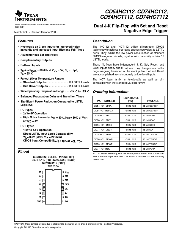
Hysteresis on Clock Inputs for Improved Noise Immunity and Increased Input Rise and Fall Times Asynchronous Set and Reset Complementary Outputs Buffered Inputs TTAyp=ic2a5lofCMAX = 60MHz at VCC = 5V, CL = 15pF, Fanout (Over Temperature Range) Wide Operating Temperature Range . . . -55oC to 125oC Balanced Propagation Delay and Transition Times Significant Power Reduction Compared to LSTTL Logic ICs HC Types - 2V to 6V Operation - High Noise Immunity: NIL = 30%, NIH = 30% of VCC at VCC = 5V HCT Types - 4.5V to 5.5V Operation - Direct LSTTL Input Logic Compatibility, VIL= 0.8V (Max), VIH = 2V (Min) - CMOS Input Compatibility, Il ≤ 1µA at VOL, VOH Pinout CD54HC112, CD54HCT112 (CERDIP) CD74HC112 (PDIP, SOIC, SOP, TSSOP) CD74HCT112 (PDIP) TOP VIEW The ’HC112 and ’HCT112 utilize silicon-gate CMOS technology to achieve operating speeds equivalent to LSTTL parts. They exhibit the low power consumption of standard CMOS integrated circuits, together with the ability to drive 10 LSTTL loads.